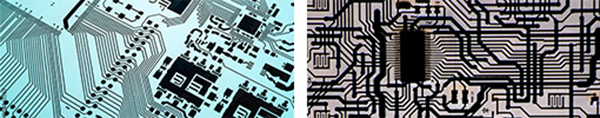
Printed electronics technology for the production of components involves materials deposited on substrates using various printing processes. Expertise and mastery of production processes are key to breaking into the printed electronics market, an industry that is evolving at an impressive pace. PRINTUP INSTITUTE is working with industrial partners ready to mass-produce electronic components for medical devices in order to breathe new life into this “Printed electronics for health and energy” ecosystem. An intra-institute working club combines its expertise to respond actively to the needs of the healthcare sector. From idea to production, the institute is involved in project management and develops partnerships with the experts needed to develop electronic components.
CLUB PRINTUP INSTITUTE
Next Club meeting: Wednesday 18 September - 10am to 5pm - Room 758
PRINTUP INSTITUTE is bringing together its partners in a club to boost the printed electronics industry dedicated to health and energy, with a view to accelerating the production of printed electronic components by French manufacturers.
A code of ethics has been drawn up to help members work together. It describes the principles and ethical values of club members. It is a tool to help everyone agree on the objectives of the institute and the duties of members. It includes a non-disclosure agreement (NDA).
A nomenclature provides an overview of the players in the printed electronics industry dedicated to health and energy, with all the stages involved in the manufacturing process. Terms of reference common to all members will be drawn up for the management of projects developed by the institute with a view to speeding up production.
Members meet four or five times a year at PRINTUP INSTITUTE to discuss current projects and develop new national or international projects.
Within the club, the institute provides a dynamic for the industry and plays a role in providing information on health expectations and marketing for its members. Club members interact on industry initiatives and recommend new operations.
ADDEV Materials is expert in high performance materials converting dedicated to hygiene and manufacturing of medical devices, supplies & hygiene specialties.
A 4.0 factory with teams of experts in electronics and multilayer screen printing, dedicated to the design and industrialization of intelligent objects linked to mobility.
Distributor of plastics, rubbers, elastomers and additives in the fields of life sciences, nutrition, coating, adhesives and silicone rubbers. Factory in France for silicone compounds.
The Laboratory of Physiochemistry of Polymers and Interfaces (LPPI) is expert in (interpenetrating) polymer networks and pi-conjugated (macro) molecules (or conductive electronic polymers).
French leader in industrial marking on various substrates (plastic and metal). Specialised for over 25 years in printed electronics, we adapt our know-how to develop the specific needs of our customers.
Expertise and innovation in printed electronics. A recognized player in the field of intelligent printed and connected objects. Production of printed electronics in France.
Development, manufacture and marketing of technical plastic films with surface functionalisation for the packaging and industrial markets. Range produced in France with PET references dedicated to printed electronics and health applications.
The university, created in 2020 on the basis of an innovative model, brings together the triptych "university/schools/research organisation" whose ambition is to transform life and cities.
Specialized in the technical and regulatory development of medical devices (class I to III) and In Vitro Diagnostic devices (class A to D).
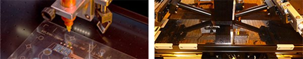
Production stages in France
PRINTUP INSTITUTE establishes the feasibility and ensures the implementation of any project. Our aim is to develop a reliable, competitive product within a controlled timeframe.
Product design
As soon as the needs of the hospital practitioner or healthcare professionals are defined, the Institute and/or its partners draw up the specifications and prepare the design of your product, taking into account your functional, ergonomic, economic and aesthetic requirements.
The development of electronic components
Promising outlets for sensors printed on flexible substrates already exist in the healthcare sector. These new applications require sensors in very large numbers and at low cost. Batteries for medical patches are thin, durable and highly flexible, and are used for niche applications such as medical patches, where their flat, compact appearance is an essential factor. Complete RFID and NFC antennas are already being mass printed. Major groups, SMEs and VSEs are already printing components in mass production. Many start-ups linked to printed electronics are creating connected products for other sectors.
IOT hardware & software integration
Today, the demand is there: the needs created by everything to do with the Internet of Things, Machine to Machine, Industry 4.0, Cloud Computing and Big Data are driving the printed electronics market. What’s new is the production of complete systems that integrate measurement, logic and energy functions. These systems will be associated with the preparation and analysis of data for the synthesis and development of products and their functionalities.
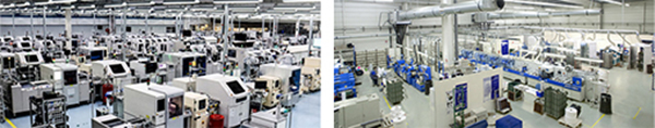
Production in France of small or large series
In the medical device industry, mass production is ready in both small and large runs. As each product is different, assembly lines are customised to optimise the case assembly and wiring process, while following specific assembly and testing procedures. Medical device manufacturers will be turning to the printed electronics industry to develop new connected objects that are flexible, practical, less expensive and offer greater functionality. All in all, a win-win situation for the patient.